Synthesis of large-area 2D material: Atomic layer pushes
surface steps away

26th April 2021by admin0

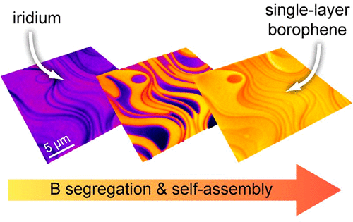
The team led by UDE’s Prof. Michael Horn-von Hoegen
aims at producing the thinnest possible layer of boron, so-called
borophene, since it promises properties that could enable the
construction of two-dimensional transistors. The molecular beam
epitaxy used for this purpose until now results in domains that are
far too small. For more precise investigations and for use in
technology, however, larger areas are needed.

Leave a Reply

Your email address will not be published. Required fields are marked *

https://nfusion-tech.com/wp-content/uploads/2019/10/Logo_newfusion-footer.png
Subscribe

If you wish to receive our latest news in your email box, just subscribe to our newsletter. We won’t spam you, we promise!

    New Fusion

    The New Fusion technology is based on a phenomenon called triplet-triplet annihilation (TTA) which is a process in which two triplet excitons annihilate and produce a higher energy singlet exciton.

    Subscribe

    If you wish to receive our latest news in your email box, just subscribe to our newsletter. We won’t spam you, we promise!

      New Fusion

      The New Fusion technology is based on a phenomenon called triplet-triplet annihilation (TTA) which is a process in which two triplet excitons annihilate and produce a higher energy singlet exciton.

      Copyright ©2024 New Fusion All Rights Reserved

      Designed by FallingBrick