Wafer-scale production of graphene-based photonic
devices

11th February 2021by admin0

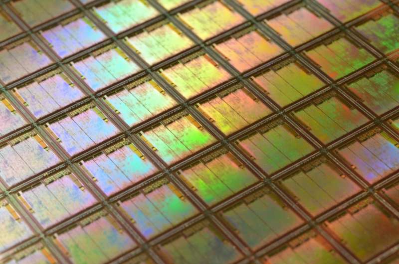
Our world needs reliable telecommunications more than
ever before. However, classic devices have limitations in terms of
size and cost and, especially, power consumption—which is directly
related to greenhouse emissions. Graphene could change this and
transform the future of broadband. Now, Graphene Flagship
researchers have devised a wafer-scale fabrication technology that,
thanks to predetermined graphene single-crystal templates, allows
for integration into silicon wafers, enabling automation and paving
the way to large scale production.

Leave a Reply

Your email address will not be published. Required fields are marked *

https://nfusion-tech.com/wp-content/uploads/2019/10/Logo_newfusion-footer.png
Subscribe

If you wish to receive our latest news in your email box, just subscribe to our newsletter. We won’t spam you, we promise!

    New Fusion

    The New Fusion technology is based on a phenomenon called triplet-triplet annihilation (TTA) which is a process in which two triplet excitons annihilate and produce a higher energy singlet exciton.

    Subscribe

    If you wish to receive our latest news in your email box, just subscribe to our newsletter. We won’t spam you, we promise!

      New Fusion

      The New Fusion technology is based on a phenomenon called triplet-triplet annihilation (TTA) which is a process in which two triplet excitons annihilate and produce a higher energy singlet exciton.

      Copyright ©2024 New Fusion All Rights Reserved

      Designed by FallingBrick