Stress-free path to stress-free metallic films paves the way
for next-gen circuitry

5th July 2021by admin0

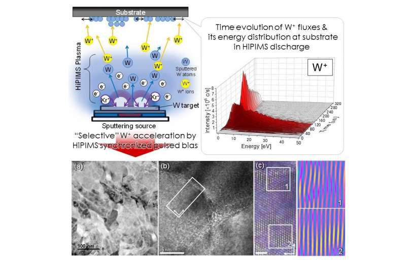
Researchers from Tokyo Metropolitan University have
used high power impulse magnetron scattering (HiPIMS) to create
thin films of tungsten with unprecedentedly low levels of film
stress. By optimizing the timing of a substrate bias pulse with
microsecond precision, they minimized impurities and defects to
form crystalline films with stresses as low as 0.03 GPa, similar to
those achieved through annealing. Their work promises efficient
pathways for creating metallic films for the electronics
industry.

Leave a Reply

Your email address will not be published. Required fields are marked *

https://nfusion-tech.com/wp-content/uploads/2019/10/Logo_newfusion-footer.png
Subscribe

If you wish to receive our latest news in your email box, just subscribe to our newsletter. We won’t spam you, we promise!

    New Fusion

    The New Fusion technology is based on a phenomenon called triplet-triplet annihilation (TTA) which is a process in which two triplet excitons annihilate and produce a higher energy singlet exciton.

    Subscribe

    If you wish to receive our latest news in your email box, just subscribe to our newsletter. We won’t spam you, we promise!

      New Fusion

      The New Fusion technology is based on a phenomenon called triplet-triplet annihilation (TTA) which is a process in which two triplet excitons annihilate and produce a higher energy singlet exciton.

      Copyright ©2024 New Fusion All Rights Reserved

      Designed by FallingBrick