Scientists shrink fin-width of FinFET to nearly the physical
limit

10th March 2020by admin0

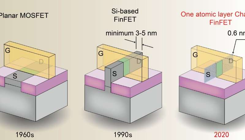
FinFETs are known to be an evolution of
metal-oxide-semiconductor field effect transistors (MOSFETs)
featuring a semiconducting channel vertically wrapped by conformal
gate electrodes. It was first proposed in 1990s in order to avoid
the short channel effect and other drawbacks resulted from the
shrinking of transistor size. Because of the limitation of
nanofabrication, the minimum fin width is about 5 nm in current
technology.

Leave a Reply

Your email address will not be published. Required fields are marked *

https://nfusion-tech.com/wp-content/uploads/2019/10/Logo_newfusion-footer.png
Subscribe

If you wish to receive our latest news in your email box, just subscribe to our newsletter. We won’t spam you, we promise!

    New Fusion

    The New Fusion technology is based on a phenomenon called triplet-triplet annihilation (TTA) which is a process in which two triplet excitons annihilate and produce a higher energy singlet exciton.

    Subscribe

    If you wish to receive our latest news in your email box, just subscribe to our newsletter. We won’t spam you, we promise!

      New Fusion

      The New Fusion technology is based on a phenomenon called triplet-triplet annihilation (TTA) which is a process in which two triplet excitons annihilate and produce a higher energy singlet exciton.

      Copyright ©2024 New Fusion All Rights Reserved

      Designed by FallingBrick