Paving a way to achieve unexplored semiconductor
nanostructures

18th October 2019by admin0

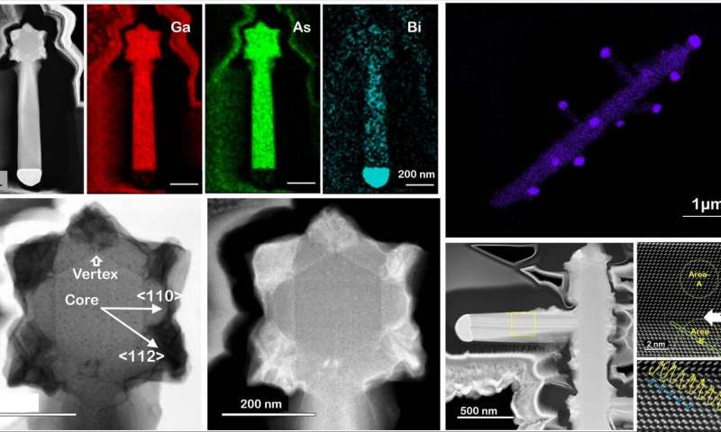
A research team of Ehime University paved a way to
achieve unexplored III-V semiconductor nanostructures. They grew
branched GaAs nanowires with a nontoxic Bi element employing
characteristic structural modifications correlated with metallic
droplets, as well as crystalline defects and orientations. The
finding provides a rational design concept for the creation of
semiconductor nanostructures with the concentration of constituents
beyond the fundamental limit, making it potentially applicable to
novel efficient near-infrared devices and quantum
electronics.

Leave a Reply

Your email address will not be published. Required fields are marked *

https://nfusion-tech.com/wp-content/uploads/2019/10/Logo_newfusion-footer.png
Subscribe

If you wish to receive our latest news in your email box, just subscribe to our newsletter. We won’t spam you, we promise!

    New Fusion

    The New Fusion technology is based on a phenomenon called triplet-triplet annihilation (TTA) which is a process in which two triplet excitons annihilate and produce a higher energy singlet exciton.

    Subscribe

    If you wish to receive our latest news in your email box, just subscribe to our newsletter. We won’t spam you, we promise!

      New Fusion

      The New Fusion technology is based on a phenomenon called triplet-triplet annihilation (TTA) which is a process in which two triplet excitons annihilate and produce a higher energy singlet exciton.

      Copyright ©2024 New Fusion All Rights Reserved

      Designed by FallingBrick