Patterning silicon at the one-nanometer scale

12th August 2021by admin0

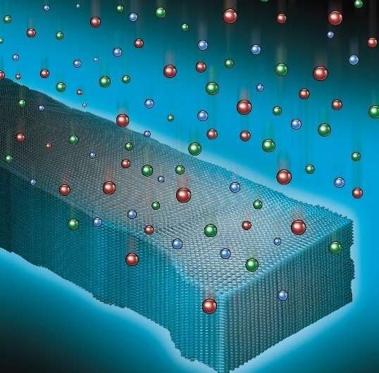
Researchers have developed an innovative technique for
creating nanomaterials. These are materials only atoms wide. They
draw on nanoscience to allow scientists to control their
construction and behavior. The new electron beam nanofabrication
technique, plasmon engineering, achieves unprecedented near-atomic
scale control of patterning in silicon. Structures built using this
approach produce record-high tuning of electro-optical
properties.

Leave a Reply

Your email address will not be published. Required fields are marked *

https://nfusion-tech.com/wp-content/uploads/2019/10/Logo_newfusion-footer.png
Subscribe

If you wish to receive our latest news in your email box, just subscribe to our newsletter. We won’t spam you, we promise!

    New Fusion

    The New Fusion technology is based on a phenomenon called triplet-triplet annihilation (TTA) which is a process in which two triplet excitons annihilate and produce a higher energy singlet exciton.

    Subscribe

    If you wish to receive our latest news in your email box, just subscribe to our newsletter. We won’t spam you, we promise!

      New Fusion

      The New Fusion technology is based on a phenomenon called triplet-triplet annihilation (TTA) which is a process in which two triplet excitons annihilate and produce a higher energy singlet exciton.

      Copyright ©2024 New Fusion All Rights Reserved

      Designed by FallingBrick