New study presents tip-induced nano-engineering of strain,
bandgap, and exciton funneling in 2D semiconductors

9th June 2021by admin0

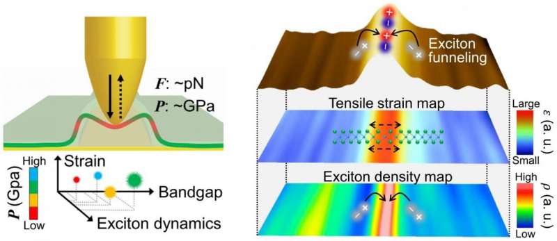
A research team, led by Professor Kyoung-Duck Park in
the Department of Physics at UNIST has succeeded in investigating
and controlling the physical properties of naturally-formed
nanoscale wrinkles in two-dimensional (2D) semiconductors. This is
thanks to their previously-developed hyperspectral adaptive
tip-enhanced photoluminescence (a-TEPL) spectroscopy. This will be
a major step forward in developing paper-thin, ultra-flexible
displays.

Leave a Reply

Your email address will not be published. Required fields are marked *

https://nfusion-tech.com/wp-content/uploads/2019/10/Logo_newfusion-footer.png
Subscribe

If you wish to receive our latest news in your email box, just subscribe to our newsletter. We won’t spam you, we promise!

    New Fusion

    The New Fusion technology is based on a phenomenon called triplet-triplet annihilation (TTA) which is a process in which two triplet excitons annihilate and produce a higher energy singlet exciton.

    Subscribe

    If you wish to receive our latest news in your email box, just subscribe to our newsletter. We won’t spam you, we promise!

      New Fusion

      The New Fusion technology is based on a phenomenon called triplet-triplet annihilation (TTA) which is a process in which two triplet excitons annihilate and produce a higher energy singlet exciton.

      Copyright ©2024 New Fusion All Rights Reserved

      Designed by FallingBrick