Nanoscale imaging of dopant nanostructures in silicon-based
devices

24th August 2020by admin0

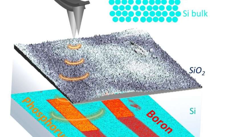
When fabricating integrated circuits and different
types of silicon-based devices, researchers need to position dopant
nanostructures in specific ways with high levels of precision.
However, arranging these structures at the nanometer scale can be
challenging, as their small size makes them difficult to observe
and closely examine. Incorrectly tampering with them can have
detrimental effects, which can potentially compromise a device’s
overall functioning and security.

Leave a Reply

Your email address will not be published. Required fields are marked *

https://nfusion-tech.com/wp-content/uploads/2019/10/Logo_newfusion-footer.png
Subscribe

If you wish to receive our latest news in your email box, just subscribe to our newsletter. We won’t spam you, we promise!

    New Fusion

    The New Fusion technology is based on a phenomenon called triplet-triplet annihilation (TTA) which is a process in which two triplet excitons annihilate and produce a higher energy singlet exciton.

    Subscribe

    If you wish to receive our latest news in your email box, just subscribe to our newsletter. We won’t spam you, we promise!

      New Fusion

      The New Fusion technology is based on a phenomenon called triplet-triplet annihilation (TTA) which is a process in which two triplet excitons annihilate and produce a higher energy singlet exciton.

      Copyright ©2024 New Fusion All Rights Reserved

      Designed by FallingBrick