Nanopatterning electronic properties of twisted 2-D
semiconductors using twist

28th May 2020by admin0

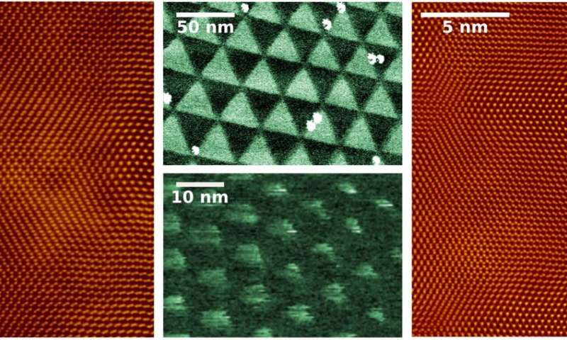
A team of researchers at the National Graphene
Institute, have demonstrated that atomic lattices of slightly
twisted 2-D transition metal dichalcogenides undergo extensive
lattice reconstruction, which can pattern their optoelectronic
properties on nanometre length scale.

Leave a Reply

Your email address will not be published. Required fields are marked *

https://nfusion-tech.com/wp-content/uploads/2019/10/Logo_newfusion-footer.png
Subscribe

If you wish to receive our latest news in your email box, just subscribe to our newsletter. We won’t spam you, we promise!

    New Fusion

    The New Fusion technology is based on a phenomenon called triplet-triplet annihilation (TTA) which is a process in which two triplet excitons annihilate and produce a higher energy singlet exciton.

    Subscribe

    If you wish to receive our latest news in your email box, just subscribe to our newsletter. We won’t spam you, we promise!

      New Fusion

      The New Fusion technology is based on a phenomenon called triplet-triplet annihilation (TTA) which is a process in which two triplet excitons annihilate and produce a higher energy singlet exciton.

      Copyright ©2024 New Fusion All Rights Reserved

      Designed by FallingBrick