Developing wafer-scale highly oriented graphene on
sapphire

1st December 2021by admin0

Researchers have used direct chemical vapor deposition
(CVD) growth of wafer-scale, high-quality graphene on dielectrics
for versatile applications. However, graphene synthesized this way
has shown a polycrystalline film with uncontrolled defects, a low
carrier mobility, and high street resistance; therefore,
researchers aim to introduce new methods to develop wafer-scale
graphene. In a new report now published in Science Advances,
Zhaolong Chen and an international research team in nanochemistry,
intelligent materials and physics, in China, U.K. and Singapore,
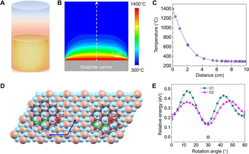
described the direct growth of highly oriented monolayer graphene
on films of sapphire wafers. They achieved the growth strategy by
designing an electromagnetic induction CVD at elevated temperature.
The graphene film developed in this way showed a markedly improved
carrier mobility and reduced sheet resistance.
Leave a Reply

Your email address will not be published. Required fields are marked *

https://nfusion-tech.com/wp-content/uploads/2019/10/Logo_newfusion-footer.png
Subscribe

If you wish to receive our latest news in your email box, just subscribe to our newsletter. We won’t spam you, we promise!

    New Fusion

    The New Fusion technology is based on a phenomenon called triplet-triplet annihilation (TTA) which is a process in which two triplet excitons annihilate and produce a higher energy singlet exciton.

    Subscribe

    If you wish to receive our latest news in your email box, just subscribe to our newsletter. We won’t spam you, we promise!

      New Fusion

      The New Fusion technology is based on a phenomenon called triplet-triplet annihilation (TTA) which is a process in which two triplet excitons annihilate and produce a higher energy singlet exciton.

      Copyright ©2024 New Fusion All Rights Reserved

      Designed by FallingBrick